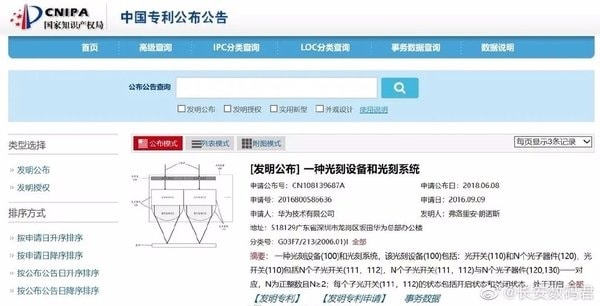
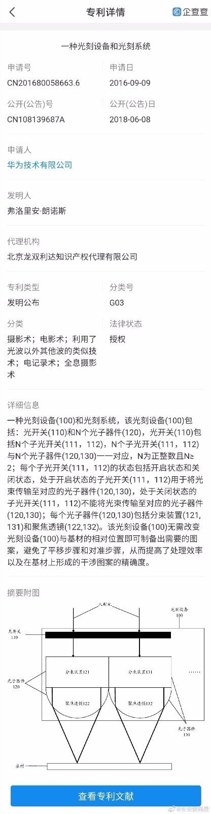
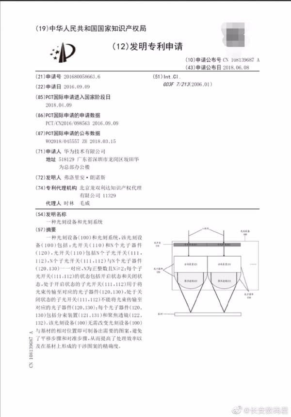
Huawei is reportedly recruiting lithography process engineers, which has sparked widespread interest. In fact, Huawei has already applied for patents for a lithography device and a lithography systems, which seem to have been prepared for the chip manufacturing process for a long time.
According to data provider Qichacha, Huawei's two patents were filed back in September 2016 and parts of them were made public in June 2018 and January 2020, respectively.
Lithography and photolithography are among the world's top technologies, and only a handful of companies worldwide have mastered the technology.
Considering that Huawei is recruiting lithography process engineers, it safe to say that Huawei does indeed have a long history of research in the chip manufacturing process.
In addition, there are reports that Huawei HiSilicon semiconductor is still in the process of expansion, is not considering scaling down.
Instead, it's actively looking for foundries to create a design and manufacturing integrated IDM.
Although Huawei HiSilicon is one of the world's top chip design companies, it is still very dependent on TSMC and a few other semiconductor companies for chip manufacturing.
Huawei's entry into the chip manufacturing field, therefore, will certainly face many difficulties, but this is also believed to be the most correct road.
It will take a long time for Huawei's IDM model to mature, and before that Huawei's various businesses will likely be looking for third-party chip supplies.
Huawei HiSilicon could have met about 80% of Huawei's mobile phone chip supply, but because of the U.S. ban, the company may have to use a lot of MediaTek chips.