The second phase of China's national memory base project started contruction yesterday in Wuhan, with a planned capacity of 200,000 wafers per month.
At the groundbreaking ceremony, Zhao Weiguo, chairman of Yangtze Memory, said that construction of the national memory base project began on December 30, 2016, with plans to build a 3D NAND flash memory chip factory in two phases, with a total investment of $24 billion.
The first phase of the project achieved a technological breakthrough and built a production capacity of 100,000 wafers/month, while the second phase has a planned production capacity of 200,000 wafers/month. The monthly production capacity totals 300,000 wafers after reaching production.
Four years ago, in 2016, China built the first phase of its National Memory Base project in Wuhan, which not only mass produced 64-layer flash memory but also saw 128-layer QLC flash memory successfully developed earlier this year.
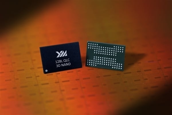
On April 13 this year, Yangtze Memory announced that its 128-layer QLC 3D flash memory (X2-) has been successfully developed. (6070) has been developed and has been validated on end products such as SSDs from multiple host manufacturers.
What makes this product unique is that it is the industry's first 128-layer QLC specification 3D NAND with a known model number. Highest storage density per unit area, highest I/O transfer speed and highest single NAND flash chip capacity in the product.
Yangtze Memory is currently ramping up its production capacity and aims to reach 100,000 wafers/month by the end of this year.