Can you imagine the arrangement that allows many football teams to train on the same court at the same time without interfering with each other? A research team in China found such a compact solution for the light waves on optoelectronic chips.
The optoelectronic chip is a cutting-edge device in the field of optical communication. When all is shut down, the large-capacity optical signal transmitted from the optical fiber is translated into an electrical signal that can be "read" by the server and the processor.
Faced with the rolling data stream, optoelectronic chips with small size and low power consumption are under great pressure in terms of bandwidth.
Harbin Institute of Technology (Shenzhen) Associate Professor Xu Ke, Professor Song Qinghai and Shanghai Jiaotong University researcher Du Jiangbing, Professor He Zuyuan teamed up to successfully design a new structure and optimization algorithm to add "lane" to the optoelectronic chip while solving crosstalk and loss to pave the way for large-scale integration.
The China Laser Magazine, sponsored by the Shanghai Institute of Optics and Fine Mechanics of the Chinese Academy of Sciences and the Chinese Optical Society, recently released the top ten developments of Chinese optics in 2019.
In an exclusive interview with a reporter from www.thepaper.cn on March 26, Xu Ke stated that this work was based on a cutting-edge "modular division multiplexing" concept and broke through key bottlenecks.
"We make large-scale integration of analog-division multiplexed photonic chips possible," he said. "At present, we have demonstrated three data channels, and the latest experimental results have completed four data channels. In the future, we will make further breakthroughs in the number of multiplexed channels and reduce the power consumption of the chip."
The gateway to photoelectric conversion
The semiconductor optoelectronic chip studied by the team is one of the communication chips that have emerged in recent years.
The basic principle of the optical communication system is this: the transmitting end modulates the electrical signal of the high-speed data stream to the optical signal output by the laser and transmits it through the optical fiber, and the receiving end receives the optical signal and then converts it into an electrical signal, which is modulated Later becomes information.
The optoelectronic chip has undertaken the task of photoelectric conversion. According to Xu Ke, large-capacity, high-data-flow optoelectronic chips have important applications in 5G front haul, data centers, and supercomputing interconnects systems.
In the future, they may also be seen in quantum computing, artificial intelligence, biosensing and other fields.
As you can imagine, the bandwidth of the optoelectronic chip is critical to the speed of the entire system. Even if the optical fiber transmission speed is faster, such as the flight time of the aircraft is very short, if there is only a line of troops when going out of the security check, it will slow down the entire journey.
Increase the "lane" of communication
The concept of analog-division multiplexing was born. It can significantly improve the parallel processing capability of the chip without increasing the number of lasers.
"Before mentioning the concept of modular division multiplexing, we must first introduce wavelength division multiplexing." Xu Ke said. Wavelength division multiplexing was proposed as early as 1978 and has been widely used in trunk fiber transmission systems.
Each data channel (waveguide) transmits several to tens of wavelengths, and each wavelength loads different data. Since the wavelengths do not interfere with each other, the communication capacity can be improved by increasing the number of wavelength channels, which is wavelength division multiplexing.
"Modular division multiplexing is similar to wavelength division multiplexing, except that another physical quantity of light waves (guided wave mode) replaces the wavelength, which adds a dimension to the multiplexing technology and is a new method to increase communication capacity." Xu Section said.
He believes that as bandwidth requirements continue to grow rapidly when wavelength resources are saturated, analog-to-multiplexing technology can further increase the bandwidth of photonic chips.
Towards large-scale integration
In recent years, people have done a lot of research on improving the bandwidth of optoelectronic chips through the use of analog-division multiplexing technology. However, a key problem that cannot be solved is the loss and crosstalk of multimode optical waveguides.
"This makes it impossible for analog-to-multiplexed chips to be routed on a large scale like integrated circuits." Xu Ke said.
In response to this problem, the research group designed a discrete waveguide superstructure, which is a new type of photonic structure that looks a bit like a two-dimensional code. With the optimization algorithm, it can achieve fine control of the light field.
The researchers designed and prepared key devices such as mode (de) multiplexers, multimode curved waveguides, and waveguide crossovers. The size is only a few microns, which is an order of magnitude smaller than traditional devices, and it is fully compatible with standard silicon optical tape flow processes.
The transmission waveguide can maintain high-efficiency and low-crosstalk signal transmission under any bending or crossing conditions.
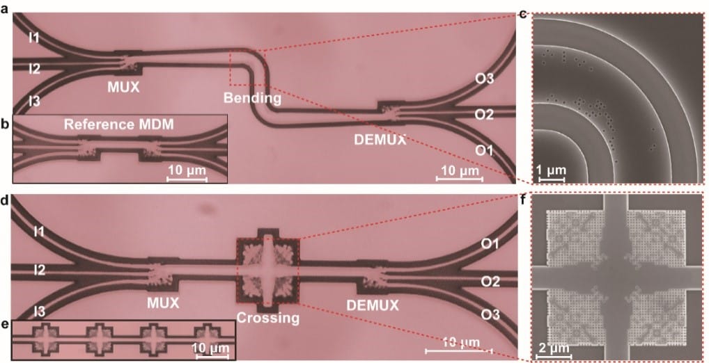
(a) Micrographs of three-mode multiplexing and curved structures; (b) Micrographs of mode multiplexing and demultiplexing devices; (c) SEM photographs of curved waveguides with sub-wavelength superstructure; (d) Three-mode multiplexing Microscope photo of the cross structure; (e) Microscope photo of the cascaded waveguide cross-device; (f) SEM photo of the waveguide cross-device with the sub-wavelength superstructure.
This new multi-mode device on the order of micrometers makes it possible to perform low-loss, low-crosstalk (de) multiplexing and arbitrary large-scale interconnection of on-chip analog-division multiplexed signals. It also provides a sophisticated optical communication device with a A new technology choice.
The global optical communication device market has grown steadily in recent years, and revenue is expected to reach US $ 16.6 billion in 2020. China has a market share of about 30%, but the R & D and manufacturing capabilities of core basic devices are relatively weak.
The "Technology Development Roadmap of China's Optoelectronic Device Industry (2018-2022)" issued by the Ministry of Industry and Information Technology proposed to ensure that the localization rate of low-end and low-end optoelectronic chips will exceed 60% and the localization rate of high-end optoelectronic chips will exceed 20% in 2022.
"High-end optoelectronic chips have always been the upstream technology that developed countries are striving to lay out, and the degree of localization in China is still very low." Xu Ke said. "We must deeply realize that we must break through the key core chip technology and get rid of the plight of missing chips."